Lab-On-Chip Devices: Materials Considerations
18 March 2024
Material selection and testing can often be one of the critical challenges to developing microfluidic devices for the healthcare and life sciences markets. Below, Springboard’s team of materials science experts summarize some of the competing material requirements that may exist for your lab-on-chip device, as well as the advantages and disadvantages of some of the processing techniques and materials that are used, along with the wide range of analytical techniques available to us to select and verify these materials.
Determining Which Physical Properties Are Needed
As with all devices that come into contact with chemical reagents and biological fluids, lab-on-chip devices have stringent material requirements. Any material used may need to be biocompatible and have good chemical resistance to any species present. Temperature stability is likely to be required for many assays – for example, up to 98 degrees C if doing PCR.
The device may be intended to interact with a variety of imaging techniques. This may necessitate low autofluorescence and transparency to optical and/or infrared wavelengths. If electrical measurements are required, the material may need particular dielectric properties.
Even more so than for traditional medical devices, the small scale can introduce unique challenges for both materials and their processing. Lab-on-chip devices can have feature sizes below standard molding tolerances, with tight tolerances on channel widths and channel high aspect ratios. These require excellent mechanical properties such as toughness, hardness, and stiffness, which should be homogeneous throughout the material. High dimensional stability is essential, which means low hygroscopicity. Conventional molding or machining routes are not suitable at this scale, so the material must be compatible with small-scale manufacturing techniques.
Finally, the small scale of features and the way they interact with fluids mean surface properties have a huge influence on the behavior of the device. The material may need to be hydrophobic or hydrophilic – or even both – in different parts of the device.
The nature of lab-on-chip devices means that they are designed and made from a small number of parts. As such, one material may be required to have all of these properties simultaneously. Achieving this may require specialized manufacturing techniques or use of surface modifications such as coatings or patterning.
Potentially Suitable Materials
Traditionally, polydimethylsiloxane (PDMS) has been used for microfluidic prototyping as it can produce fine surface details quickly using a cold casting process. However, it is generally not suitable for commercial applications due to, among other things, its mechanical properties and tendency to absorb small hydrophobic molecules. New soft, thermoplastic elastomers are emerging that can be used to replace PDMS.
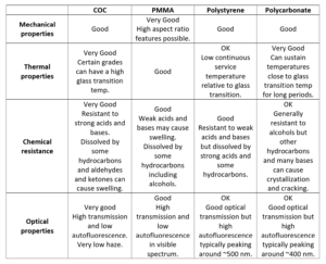
A range of engineering thermoplastic polymers can also be used for LOC applications, including poly(methyl methacrylate) (PMMA), polystyrene (PS), polycarbonate (PC), or cyclic olefin copolymer (COC). These are optically transparent, generally resistant to a range of chemicals, and compatible with a wide range of manufacturing and joining techniques, making them ideal choices. Some of the relative advantages and disadvantages of these materials are summarized below.

Table 1: Properties of engineering polymers commonly used in lab-on-chip devices
Where polymers are not suitable for reasons of chemical compatibility, glass and silicon are alternative options. These can be machined or patterned using well-established wet- or dry-lithography techniques but are typically more expensive than polymers.
Finally, there is growing awareness of the environmental impact of disposable lab-on-chip devices and, consequently, growing interest in more sustainable alternatives. These may include biopolymers such as poly(lactic acid) (PLA) and polyhydroxybutyrate (PHB), or even paper. Paper-based microfluidics have long been used for simple lateral-flow assays, but Springboard has more recently seen devices making use of multiple layers and colorimetry to add complexity to assays while keeping costs low.
Processing Techniques
Cold casting
Lab-on-chip prototypes are often made from polydimethylsiloxane by cold casting. This transparent polymer is cast from a two-part mixture at low temperatures over a mold. The molds themselves can be machined or 3D-printed for rapid iteration. Reproduction of small features and surface textures can be excellent, so the limit to the quality of the casting is the ability to produce a mold with small features and a smooth surface. For improved precision and low surface roughness, a lithography process may be used to make a mold from silicon or glass.
Micromachining and laser ablation
Some devices can be prototyped by direct machining using conventional drilling and milling techniques. While these may seem attractive due to their flexibility and the potential for rapid design and test iterations, their suitability for such small-scale devices is questionable. They are time-consuming, the resolution is limited, and they are prone to leaving a poor surface finish that affects the functionality of the device.
An alternative to conventional micromachining is laser ablation, suitable for some materials such as PMMA but not widely used for other polymers. A high-intensity laser is used to ablate material at the focal point, leading to less surface roughness, but costs and limited material choices mean this technique is not as widely used.
3D printing
Increasingly, 3D printing is becoming an option for prototyping microfluidic devices. Improving resolutions mean it is now possible to print features down to low hundreds of microns and using something like a COC filament allows for rapid iterations in materials that are representative of those that would be used in a commercial device.
Thermal forming – injection moulding and hot embossing
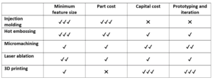
An option for scale-up to mass manufacture is thermal forming of polymers, either by injection molding or by hot embossing into a flat sheet. Once optimized, either technique can yield excellent surface reproduction at arbitrarily high production volumes. However, molds and embossing tools for these techniques are typically machined from steel, so the up-front capital costs are high. Many companies will prototype with other techniques and then transfer to a contract manufacturer for high-volume production.

(✔✔✔ = excellent; ✔✔ = good; ✔ = acceptable; ✖ = poor)
Table 2: Comparison of processing techniques for polymers in lab-on-chip devices.
Analytical Techniques
The small scale of lab-on-chip devices and the consequent dependence of device functionality on material and surface properties means that conventional inspection techniques may not be sufficient to qualify components and production processes. A suite of appropriate techniques may be necessary, for example:
- Dimensional tolerances can be assessed using optical coordinate measurement. One hundred percent inspection is unlikely to be possible, so statistical process control techniques are used to demonstrate adherence to tolerances.
- Mechanical properties of materials can be easily measured at the bulk scale, but specialist techniques such as microindentation or micromechanical testing may be required to probe small features of the design.
- Coating adherence can be measured using microindentation or micro-scratch testing. Scanning electron microscopy (SEM) can also be informative, particularly in the analysis of fracture and delamination failures.
- Surface roughness is critically important to cell growth and hydrophilicity, as well as to the optical properties of a device. It can be quantified using optical profilometry or atomic force microscopy (AFM).
- Surface properties such as surface energy and hydrophilicity are typically measured using contact angle measurements, which can even be time-resolved to capture transient behaviors. The small scales involved in lab-on-chip devices may require specialist picoliter dropping equipment.
- Chemical properties, including leaching of unwanted chemicals from adhesives or other precursors, can be detected using a range of techniques including high-performance liquid chromatography (HPLC) or infrared spectroscopy.
Approach To Working With Challenging Materials Requirements
Given the stringent requirements on materials discussed at the start, how can these materials and techniques be used to create a successful lab-on-chip device? In Springboard’s experience, the key factors that will lead to success are:
- Know your requirements. Crucially, as well as technical requirements, this needs to include regulatory, processing, and commercial requirements from as early as possible.
- Consider the likely final manufacturing processes from the beginning. Fundamental decisions made early in the design process can limit the material and processing options available to you. For example, if your final device needs to be made in millions, consider whether your design could be produced by a low-cost process such as injection molding or die cutting.
- Use processes that allow you to iterate quickly to get your design working, but make sure you stick to the design rules of the volume process. 3D printing, PDMS, and CNC machining are great, but don’t do all your testing with a design that then needs to be changed. Stick to channel widths, aspect ratios, and geometries feasible for the final device.
- Use analytical techniques to understand the details of material interactions, including differences between prototypes and production. Techniques like those listed above can be extremely illuminating and give you confidence that you can achieve reliable performance in production.
As featured in Med Device Online
Written by Philip Howie Ph. D and Adam Nightingale


